20%
+R&D investment/revenue


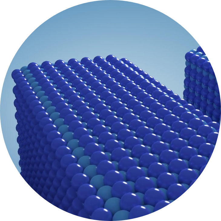
Atomic Layer Deposition (ALD) technology:
Have:
Three-dimensional conformability, widely applicable to different shapes of substrates.
Uniformity of film formation over large areas with dense, pinhole-free films
Sub-nanometer film thickness control
Precise control of nanostacking and atomic doping ratios


Video Playback
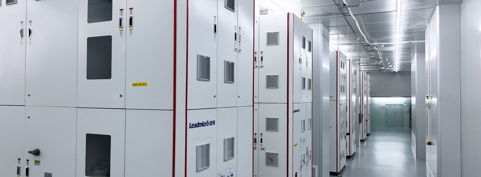
R&D Innovation

20%
+R&D investment/revenue

56200
㎡Production and R&D bases

3000
+Proprietary technology (item)

35%
+Percentage of R&D staff

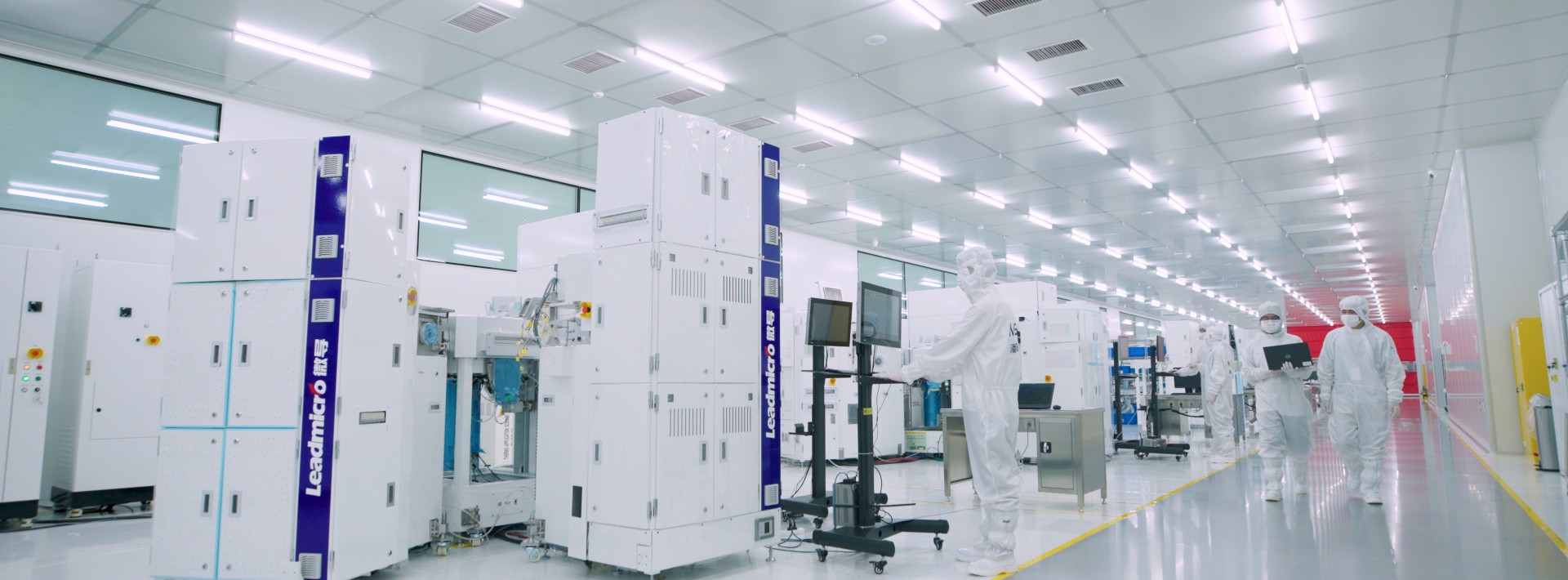
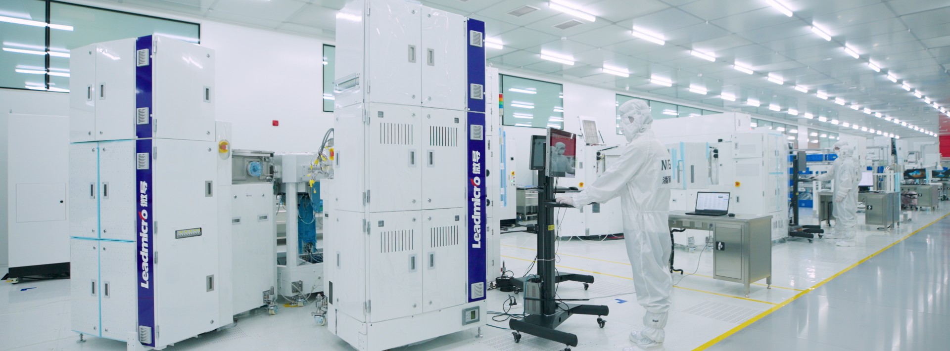


Core Technical Team
Professional Team
Process Development

Specialized ALD manufacturers
Professional ALD
Professional Solutions

Domestic leading forward-looking application customization
Forward-looking applications
Custom development

The only full-scene demo equipment line in China
Full Scene Demo
Mass production experience


Intellectual Innovation
Semiconductor equipment planning capacity
Planned capacity of photovoltaic equipment


Service Innovation